We are defining
the future of sensing
Unparalleled control, performance, and new information from a single flat lens. Optics made in any semiconductor foundry to empower billions of devices in the real world.


Unlock the unseen
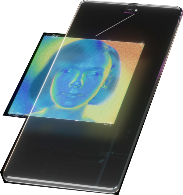
Meet Polar ID, a full system solution for smartphone biometrics and beyond.
Benefits of Meta-Optics
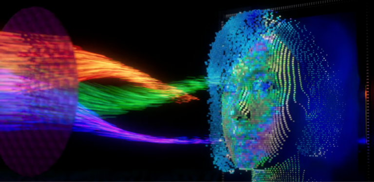
Simplifying complex optical modules to enable new information in mass markets. Multiple optical functions implemented in a single, flat optic allow for complete control of all information in light. Our optics bring the precision of the semiconductor foundries and optics together for the first time.
What are Meta-Optics 
Core Markets